Computational materials science research group
2025

![]()
![]()
![]()
![]()
![]()
Density Functional Theory and its application to the computational simulation and modeling of optical, vibrational, electronic and thermoelasic properties of materials.
![]()
Research Areas

1.
Rahul Trivedi, Po-Liang Liu, Radek Roucka, John Tolle, A.V.G.
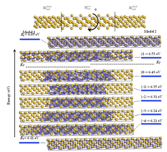
Chizmeshya, I. S. T. Tsong and J. Kouvetakis*, ”Mismatched
Heteroepitaxy of Tetrahedral Semiconductors with Si via ZrB2
Templates”, Chemistry of Materials, Vol. 17, No.18,
pp.4647-4652, 2005.
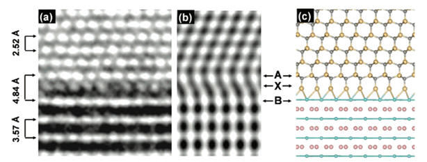
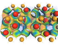
Comparison of the observed (a) and simulated (b) XTEM
micrographs of the SiC-ZrB2 interface microstructure. The
simulated XTEM pattern (b) was obtained from the ab initio
interface structure corresponding to the lowest energy model A.
This comparison suggests that the transition layer (X), above,
consists of silicon atoms bonded to adjacent Zr and C atomic
rows as shown in model structure c. Yellow, black, blue and pink
spheres represent the atoms Si, C, Zr and B, respectively.
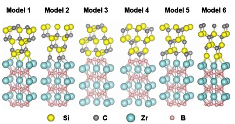
2.
Po-Liang Liu, A. V. G. Chizmeshya, John Kouvetakis, and Ignatius
S. T. Tsong*, “First-Principles Studies of GaN(0001)
Heteroepitaxy on ZrB2(0001)”, Physical Review B, Vol. 72,
pp.245335, 2005.
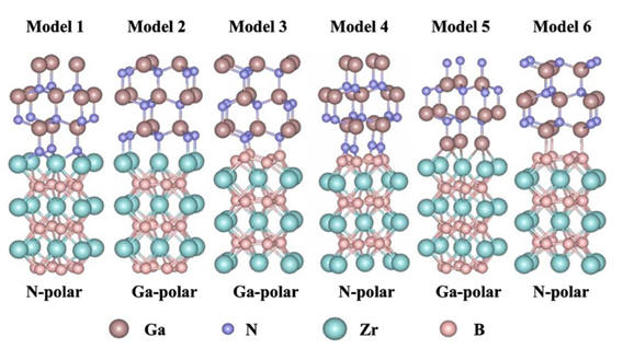
Atomistic representations of the six GaN(0001)/ZrB2(0001) relaxed interface models fixed at the sto- ichiometry of Ga6N6Zr6B12. The atoms are represented by spheres: Ga brown, large , N dark blue, small , Zr light blue, large , and B pink, small . Models 1, 4, and 6 have N-polar GaN surfaces, while models 2, 3, and 5 have Ga-polar GaN surfaces.
3. T. Wang, Y. Yamada-Takamura, Y. Fujikawa, T. Sakurai, Q. K.
Xue, J. Tolle, P.-L. Liu, A. V. G. Chizmeshya, J. Kouvetakis,
and I.S.T. Tsong*, “Surface and interface studies of GaN epitaxy
on Si(111) via ZrB2 buffer layers”, Physical Review Letters,
Vol. 95, pp.266105, 2005.
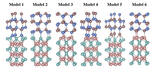
Atomistic representations of the six GaN(0001)/ZrB2(0001)
interface models. The atoms are repre- sented by spheres: Ga
(brown), N (dark blue), Zr (light blue), and B (pink). Models 1,
4, and 6 are N-polar, while models 2, 3, and 5 are Ga-polar.
4.
Po-Liang Liu, A. V. G. Chizmeshya*, and John Kouvetakis,
“Structural, Electronic and Energetic Properties of SiC[111]/ZrB2[0001]
Heterojunctions: A First Principles DFT Study”, Physical Review
B, Vol. 77, pp.035326, 2008.
Ball and stick structural representations of the six interface configuration models considered in this study.
5.
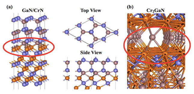
Po-Liang Liu*, “Highly Strained Metastable Heterojunction
between Wurtzite GaN(0001) and Cubic CrN(111)”, Journal of The
Electrochemical Society, Vol. 157, pp. D577-D581, 2010.
6.
Po-Liang Liu* and Yu-Jin Siao, “Ab initio study on preferred
growth of ZnO”, Scripta Materialia, Vol. 64, pp. 483-485, 2011.
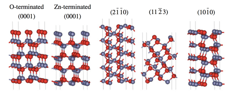
Atomistic representations of the five ZnO surface models. The
atoms are represented by spheres: O, red; Zn, light gray.
7.
Po-Liang Liu*, Yu-Jin Siao, Yen-Ting Wu, Chih-Hao Wang and Chien-Shun
Chen, “Structural, electronic and energetic properties of GaN[0001]/Ga2O3[100]
heterojunctions: A first-principles density functional theory
study”, Scripta Materialia, Vol. 65, pp. 465-468, 2011.
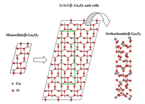
An orthorhombic b-Ga2O3 lattice representation comprising 16 Ga and 24 O atoms constructed from a center of a 3 X 3 X 3 repeat of the basic monoclinic b-Ga2O3 unit cell (green rectangle). Ga and O atoms are represented by brown and red spheres, respectively. (For interpretation of the references to color in this figure legend, the reader is referred to the web version of this article.)
8.
Yu-Jin Siao, Po-Liang Liu*, and Yen-Ting Wu, “Ab initio Study of
Atomic Hydrogen on ZnO Surfaces”, Applied Physics Express, Vol.
4, pp. 125601, 2011.
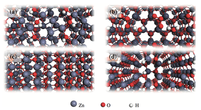
9.
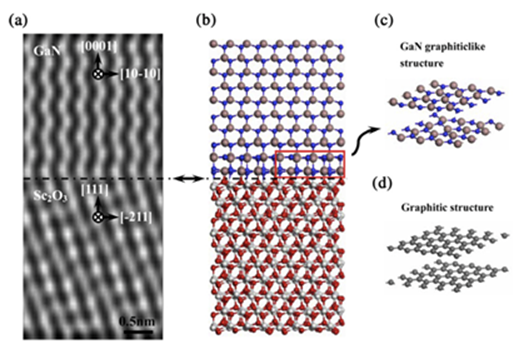
Po-Liang Liu* and Kuo-Cheng Liao, “Accommodation at the
interface of highly dissimilar GaN(0001)/Sc2O3(111)
heteroepitaxial systems”, Scripta Materialia, Vol. 68, pp.
211-214, 2013.
10.
Po-Liang Liu*, Yen-Ting Chou, and Jia-Yang Hong, “Valence-Band
Offset of m-Plane GaN(1100) Films Grown on LiAlO2(100)
Substrates”, Applied Physics Express, Vol. 6, pp. 071001, 2013.
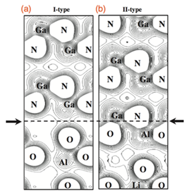
Valence charge density maps corresponding to (a) I-type and (b) II-type interface structural models, respectively. The contours are plotted in the range from 0.018 to 0.288 electrons/A3 in 16 steps. The arrows indicate the position of the interface.
11.
Yen-Wei Chen, Po-Liang Liu*, and Chun-Hsiang Chan,
“First-Principles Studies of Er2O3(110) Heteroepitaxy on
Si(001)”, International Journal of Applied Physics and
Mathematics, Vol. 4, pp. 108–112, 2014.
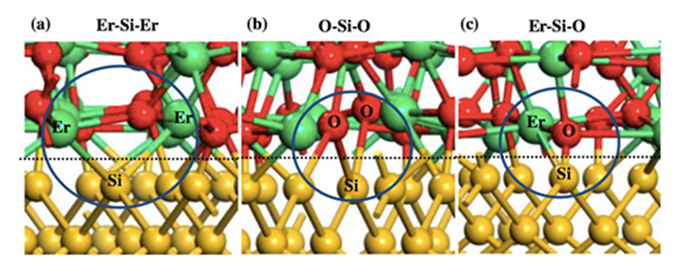
Ball and stick structural representations of (a) Er–Si–Er, (b)
O–Si–O, and (c) Er–Si–O bonding environments on Er2O3/Si
interfaces considered in this study. The dashed line is the
interface. The atoms are represented by spheres: Er (green,
large), O (red, small), and Si (yellow, medium).
12.
Cheng-Lun Hsin, Hsu-Shen Teng, Hsiang-Yuan Lin, Tzu-Hsuan Cheng,
Chao- Chia Cheng, and Po-Liang Liu, ”Electronic structure and
infrared light emission in dislocation-engineered silicon”, IEEE
Transactions on Nanotechnology, Vol. 14, pp. 399-403, 2015.
13.
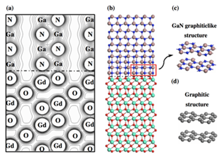
Kuo-Cheng Liao, Yu-Hsien Wang, Po-Liang Liu*, and Huan-Chen
Wang, “Fundamental properties of GaN(0001) films grown directly
on Gd2O3(0001) platforms: ab initio structural simulations”,
Optical and Quantum Electronics, Vol. 48, pp.198, 2016.
14.
Ray-Hua Horng*, Chiung-Yi Huang, Sin-Liang Ou, Tzu-Kuang Juang,
and Po-Liang Liu, “ Epitaxial Growth of ZnGa2O4: A New Deep
Ultraviolet Semiconductor Candidate”, Crystal Growth & Design ,
Vol. 17, pp. 6071-6078, 2017
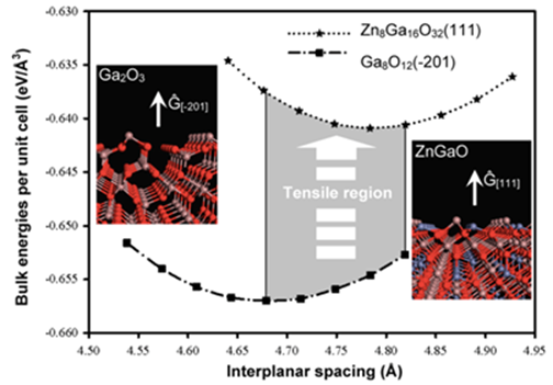
Bulk energies per unit cell of Ga8O12(2̅01) and Zn8Ga16O32(111)
as a function of interplanar spacings. The shade region
indicates the tensile region leads to more unfavorable Ga8O12
and more favorable Zn8Ga16O32 structures. The atoms are
represented by spheres: Ga (brown, large), Zn (purple, middle),
and O (red, small).
15.
Li-Chung Cheng, Min-Ru Wu, Chiung-Yi Huang, Tzu-Kuang Juang,
Po-Liang Liu, and Ray-Hua Horng*, “ Effect of Defects on the
Properties of ZnGa2O4 Thin-Film Transistors”, ACS Applied
Electronic Materials, Vol. 1, pp. 253-259, 2019
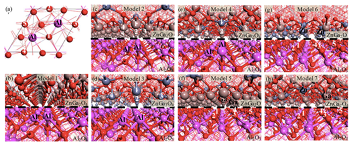
Representative interfaces of the optimized structural ZnGa2O4 grown on (0001) sapphire substrates, corresponding to an (a) in-plane view of model 1, (b) six O−Al bonds in model 1, (c) six Ga−Al bonds in model 2, (d) six Zn−Al bonds in model 3, (e) four Ga−Al and two Zn− Al bonds in model 4, (f) six Ga−O bonds in model 5, (g) six Zn−O bonds in model 6, and (h) three Ga−O and Zn−O bonds in model 7 interfaces indicated by the dashed lines. The atoms are represented by spheres: Zn (purple, medium), Ga (brown, large), O (red, small), and Al (pink, medium).
16.
Ming-Chun Tseng, Dong-Sing Wuu, Chi-Lu Chen, Hsin-Ying Lee,
Cheng-Yu Chien, Po-Liang Liu, and Ray-Hua Horng*,
“Characteristics of atomic layer deposition–grown zinc oxide
thin film with and without aluminum”, Applied Surface Science,
Vol. 491, pp. 535–543, 2019.
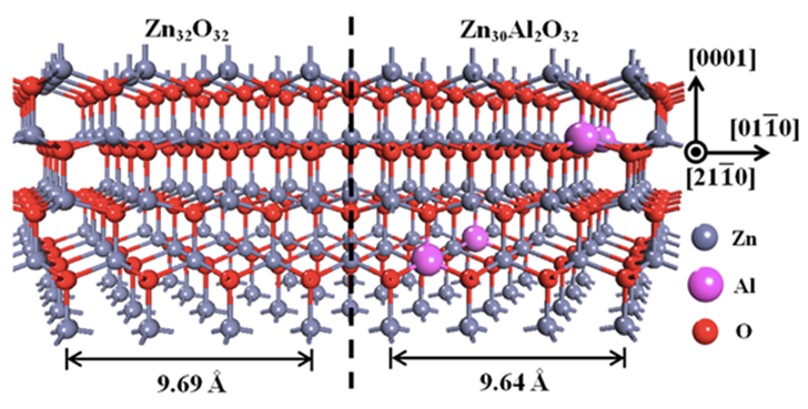
Illustration of the ZnO/AZO interface re- sulting in a small
lattice mismatch of 0.5% de- termined using relaxed optimized
Zn32O32 and Zn30Al2O32 structures. Atoms are represented by
spheres: O (red, small), Zn (gray, medium), and Al (pink,
large). (For interpretation of the references to color in this
figure legend, the reader is referred to the web version of this
article.)